← 4 Stroke Engine Diagram: How Your Engine Really Works! Four 4 number · free image on pixabay MX19 Scissor Lift Wiring Diagram: Operate Safely & Smartly! [diagram] jlg wiring diagram scissor lift →
If you are looking for Via-filling Plating in PCB Manufacturing Process you've came to the right place. We have 25 Pictures about Via-filling Plating in PCB Manufacturing Process like Detailed Procedures of Plating Copper for PCB Processing - PCB, Detailed Procedures of Plating Copper for PCB Processing - PCB and also The Ultimate Guide to Understanding Via Plating Thickness in PCBs - Top. Here it is:
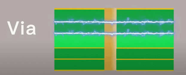
Via-filling Plating In PCB Manufacturing Process
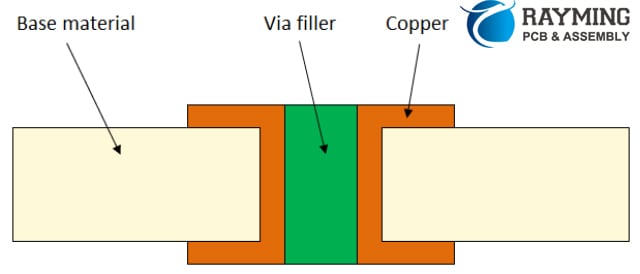 www.raypcb.com
Via-filling Plating in PCB Manufacturing Process
Inspirasi Pcbway Via Plating Thickness Skema Pcb - Vrogue.co
 www.vrogue.co
Inspirasi Pcbway Via Plating Thickness Skema Pcb - vrogue.co
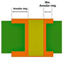
The Ultimate Guide To Understanding Via Plating Thickness In PCBs - Top
 camtechpcb.com
The Ultimate Guide to Understanding Via Plating Thickness in PCBs - Top ...
The Ultimate Guide To Understanding Via Plating Thickness In PCBs - Top
 camtechpcb.com
The Ultimate Guide to Understanding Via Plating Thickness in PCBs - Top ...
Detailed Procedures Of Plating Copper For PCB Processing - PCB
 www.pcbway.com
Detailed Procedures of Plating Copper for PCB Processing - PCB ...
Pcb Design - PCB Base Copper Weight Vs Plating Thickness - Electrical
 electronics.stackexchange.com
pcb design - PCB base copper weight vs plating thickness - Electrical ...
Why Some PCBs Need Edge Plating? - Technology - PCBway
 www.pcbway.com
Why Some PCBs Need Edge Plating? - Technology - PCBway
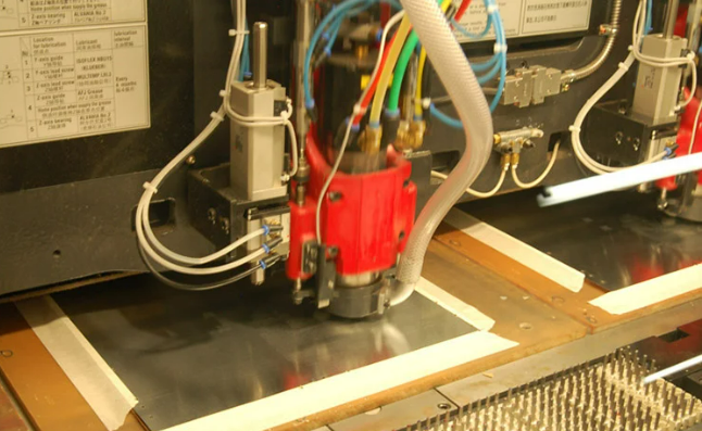
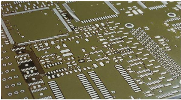
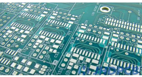
PCB Manufacturing Process & Equipment - PCBWay
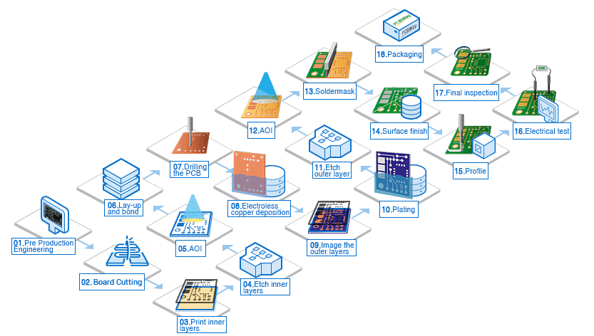 www.pcbway.com
PCB manufacturing Process & Equipment - PCBWay
Double-sided PCB Manufacturing Process Flowchart And Step By Step
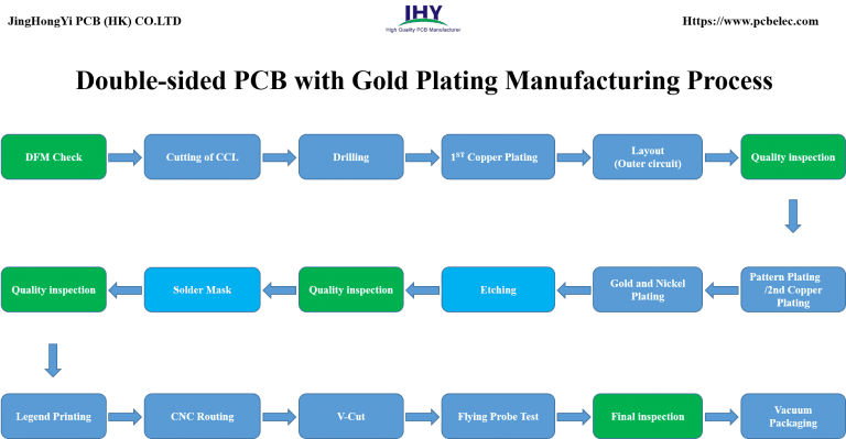 www.pcbelec.com
Double-sided PCB Manufacturing Process Flowchart and Step by Step
PCB Plating: The Complete Guide Of Plating Techniques In PCB
 www.wellpcb.com
PCB Plating: The Complete Guide of Plating Techniques in PCB
Pcb Design - PCB Base Copper Weight Vs Plating Thickness - Electrical
 electronics.stackexchange.com
pcb design - PCB base copper weight vs plating thickness - Electrical ...
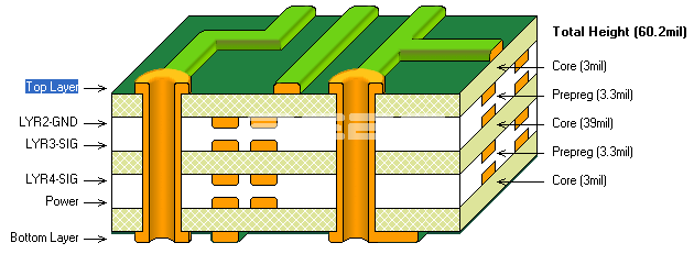
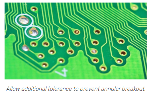
Pcb Tolerances Pcb Thickness Standards Advanced Circu - Vrogue.co
 www.vrogue.co
Pcb Tolerances Pcb Thickness Standards Advanced Circu - vrogue.co
Via-in-Pad In PCB Design Manufacturing | Sierra Circuits
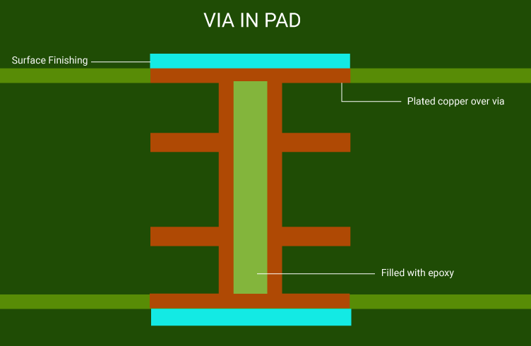 www.protoexpress.com
Via-in-Pad in PCB Design Manufacturing | Sierra Circuits
The Ultimate Guide To Understanding Via Plating Thickness In PCBs - Top
 camtechpcb.com
The Ultimate Guide to Understanding Via Plating Thickness in PCBs - Top ...
Copper Wrap Plating For PCB Manufacturing | Sierra Circuits
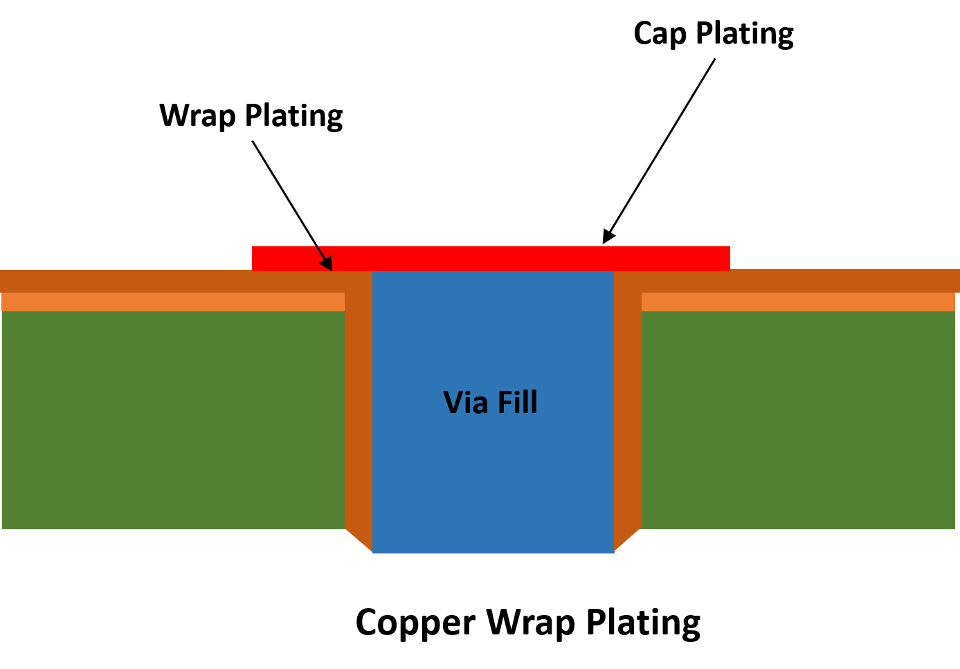 www.protoexpress.com
Copper Wrap Plating for PCB Manufacturing | Sierra Circuits
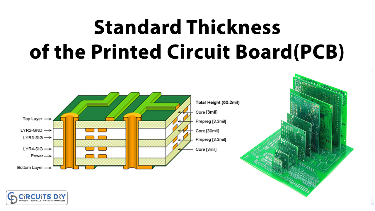
Standard Pcb Thickness Chart
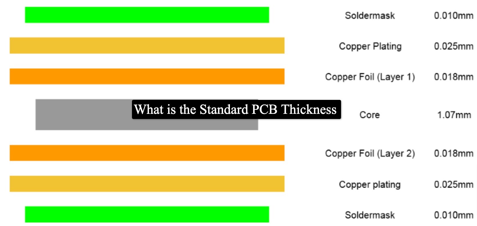 mavink.com
Standard Pcb Thickness Chart
Detailed Procedures Of Plating Copper For PCB Processing - PCB
 www.pcbway.com
Detailed Procedures of Plating Copper for PCB Processing - PCB ...
The Ultimate Guide To Understanding Via Plating Thickness In PCBs - Top
 camtechpcb.com
The Ultimate Guide to Understanding Via Plating Thickness in PCBs - Top ...
PCB & PCB Assembly Reviews - Share - PCBWay
 www.pcbway.com
PCB & PCB Assembly Reviews - share - PCBWay
The Ultimate Guide To Understanding Via Plating Thickness In PCBs - Top
 camtechpcb.com
The Ultimate Guide to Understanding Via Plating Thickness in PCBs - Top ...
Selective Gold Plating PCBs Manufacturers | FX PCB
 sfxpcb.com
Selective Gold Plating PCBs Manufacturers | FX PCB
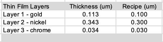
Plating Thickness Measurements - SEM Lab Inc.
 www.semlab.com
Plating Thickness Measurements - SEM Lab Inc.
The Ultimate Guide To Understanding Via Plating Thickness In PCBs - Top
 camtechpcb.com
The Ultimate Guide to Understanding Via Plating Thickness in PCBs - Top ...
PCB Via Plating: Depth Guide And Process - Jhdpcb
 jhdpcb.com
PCB Via Plating: Depth Guide And Process - Jhdpcb
The Ultimate Guide To Understanding Via Plating Thickness In PCBs - Top
 camtechpcb.com
The Ultimate Guide to Understanding Via Plating Thickness in PCBs - Top ...
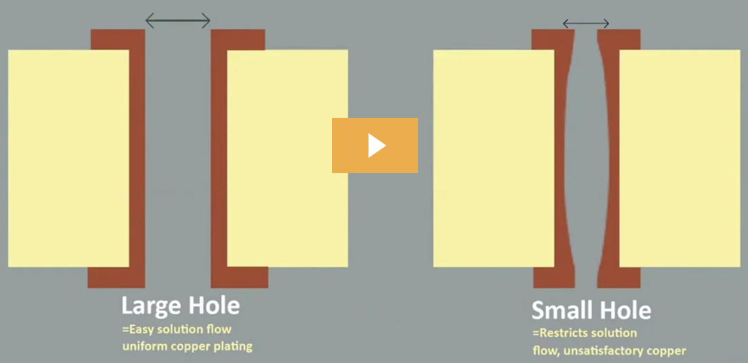
The ultimate guide to understanding via plating thickness in pcbs. Double-sided pcb manufacturing process flowchart and step by step. pcb via plating: depth guide and process